SOI-Wafer (Silicon on Insulator)

We have many years of experience in SOI technology. High performance makes them the product of choice for special applications. We can meet your individual requirements even in small quantities. We will be happy to advise you on the right specifications for your application.

Please call us on +49-(0)8191-478747 or contact us by e-mail.

We can offer you the following SOI wafers

SOI (Silicon on Insulator)

Fusion-Bonded

SOI refers to a special insulating layer field effect transistor. Here, a thin silicon layer is separated from the silicon substrate by an insulating layer (Buried-Thermal-Oxide, BOX). This layer structure offers improved electrical insulation, reduced parasitic capacitance and enables higher performance of integrated circuits and other semiconductor components.

Structure of SOI wafers

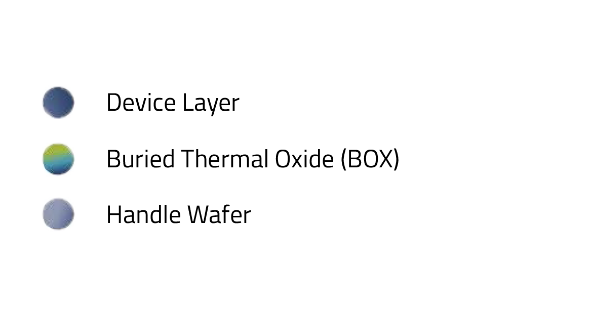
An SOI wafer typically consists of three main layers:

Device Layer:
The top layer of the SOI wafer consists of a thin layer of high-purity silicon that serves as the active area for the manufacture of semiconductor devices. This silicon layer can normally have thicknesses ranging from a few nanometers to a few micrometers, depending on the requirements of the application.

Buried Thermal Oxide (BOX):
Underneath the active silicon layer is an insulating layer, usually made of silicon dioxide (SiO2). This insulating layer separates the active silicon layer from the underlying substrate and prevents electrical interactions and leakage currents between the layers.

Handle wafer:
The lowest substrate of the SOI wafer consists of a silicon substrate that serves as a mechanical support and structural base for the thin layers. The carrier substrate can usually have a standard silicon wafer structure.

Areas of application for our SOI wafers (Silicon on Insulator):

Semiconductor industry

SOI wafers are used in semiconductor manufacturing to produce high-performance and energy-efficient integrated circuits (ICs). The insulating layer (insulator) between the top silicon layer and the silicon substrate reduces parasitic capacitance and improves the switching speed and energy efficiency of ICs.

Optoelectronics

In optoelectronics, SOI wafers are used for the production of optical components such as optical modulators, photonic integrated circuits and optical sensors. The SOI structure enables precise control of light and provides a platform for the integration of optical and electronic components on one chip.

High-frequency and high-performance electronics

SOI wafers are also used in high-frequency and high-power electronics, for example in the manufacture of high-frequency circuits, high-power amplifiers and RF components. The SOI structure enables better insulation between the components and reduces interference and losses in the circuits.

MEMS (microelectromechanical systems)

SOI wafers are also used in MEMS technology to produce microelectromechanical systems such as pressure sensors, accelerometers, gyroscopes and micromotors. The SOI structure enables precise mechanical movements and sensor operations due to the insulated silicon layer.

Typical SOI wafer specifications:

Diameter:
76,2mm
100mm
125mm
150mm
200mm

Device Layer:
1,5μm – 600μm

BOX-Layer:
10nm – 10μm

Handle Layer:
300μm – 2000μm

Bonding Method:
Fusion-Bonded

Handle Wafer:
Diameter: 76,2 mm – 200mm
Type/Dopant: P/Bor, N/Phos, N/Sb, N/As, Undoped, Intrinsic
Orientation: <100>, <111>, <110>
Resistivity: 0,001 – 50,000ohmcm
Edge Exclusion: 5 mm
Surface Finish: SSP, DSP