Silicon Wafers

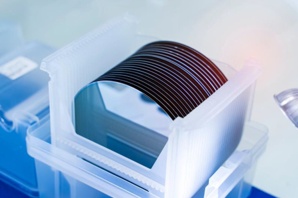
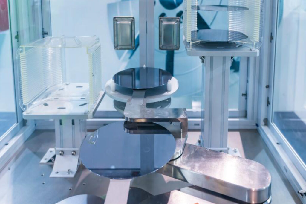
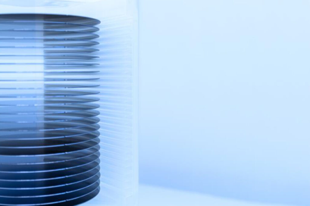
We offer you silicon wafers with almost any specification from leading international wafer manufacturers. Our high-purity wafers are grown using the Czochralski process (CZ) or the float zone process (FZ). With our highly specialized finishing options, we can meet your individual requirements. Small quantities can also be processed.

We will be happy to advise you on the right specifications for your application.

Please call us on +49-(0)8191-478747 or contact us by e-mail.

We can offer you these types of silicon wafers

Standard wafers 25.4mm – 300mm

Thanks to our large stocks, we can guarantee you rapid availability of 50.8mm to 300mm wafers in large quantities. This enables us to avoid supply bottlenecks and reliably supply you with standard wafers at all times.

Customized products

For over 20 years, we have specialized in the custom production of silicon wafers. In cooperation with long-standing partners, we can offer you extensive specifications.

SEMI International Standards

2“ Std WaferCZ, 50,8mm, 280μm, P/Bor, <100>, 1-30ohmcm, SSP, 1 Flat SEMI
3“ Std WaferCZ, 76,2mm, 380μm, P/Bor, <100>, 1-30ohmcm, SSP, 2 Flat SEMI
4“ Std WaferCZ, 100mm, 525μm, P/Bor oder N/Phos, <100>, 1-30ohmcm, SSP, 2 Flats SEMI
6“ Std WaferCZ, 150mm, 675μm, P/Bor oder N/Phos, <100>, 1-30ohmcm, SSP, 2 Flats SEMI
8“ Std WaferCZ, 200mm, 725μm, P/Bor, <100>, 1-5ohmcm, SSP, Notch SEMI
12“ Std WaferCZ, 300mm, 775μm, P/Bor, <100>, 1-100ohmcm, DSP, Notch SEMI

FZ / CZ wafers

FZ (Floating Zone) and CZ (Czochralski) wafers represent different manufacturing methods for silicon wafers. FZ wafers are produced by melting and recrystallizing silicon, while CZ wafers are obtained by slowly pulling a silicon crystal from a silicon melt. From a silicon melt, whereby defined crystal orientations and doping profiles can be achieved.

Prime wafers

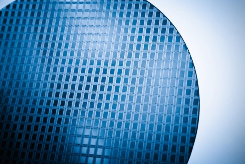
Prime wafers are newly manufactured, high-purity silicon wafers that are used for the production of integrated circuits (ICs), microprocessors, microcontrollers, memory chips, electronic components and other high-quality semiconductor products. They are specified according to SEMI standards and are characterized by high quality, low defect numbers and a precise surface finish. Individual parameters (particles, TTV, etc.) can have even better and more precise tolerances than the SEMI standards, depending on customer requirements and focus.

Test wafers

Test wafers are manufactured specifically for testing and development activities. Test wafers have larger tolerances in the material properties or minor defects, as they are primarily intended for test purposes and not for mass production.

Reclaim wafers

Reclaim wafers are remanufactured wafers that are obtained from surplus prime wafers. These wafers undergo a special process to remove defects and restore the surface quality.

Areas of application for our silicon wafers

Semiconductor industry

Silicon wafers are used for the production of various integrated circuits, including memory chips and logic circuits. The semiconductor industry is fundamental to electronics production and digital technologies.

Microprocessors and microcontrollers

Silicon wafers form the basis for the production of microprocessors and microcontrollers, which are used in computers, smartphones and other electronic devices. These applications are crucial to the functionality and performance of modern electronics.

Optoelectronics and sensor technology

Silicon wafers are used in the manufacture of image sensors, optoelectronic components and sensors. These applications are present in cameras, lighting technology, vehicles and many other areas.

MEMS (microelectromechanical systems)

Silicon wafers serve as a platform for the production of MEMS, which are used in sensors, actuators and small mechanical systems. MEMS are used in areas such as medical technology, aerospace and consumer electronics.

Typical silicon wafer specifications:

Diameter:
25,4mm
50,8mm
76,2mm
100mm
125mm
150mm
200mm
300mm

Grade:
Prime
Test
Reclaim

Type/Dopant:
P/Bor
N/Phos
N/Sb
N/As
Undoped
Intrinsic

TTV:
< 5μm
< 1μm (ultra flat)

Bow/Warp:
< 30μm

Flat/Notch:
SEMI Std.
No Flat
2 Flat
2 Flats
Jeida Flat
Notch

Surface/ Finish:
SSP
DSP
As cut
Lapped
Etched

Thickness:
50 – 8,000μm

Growth:
CZ (Czochralski)
FZ (Floating Zone)

Orientation:
<100>
<111>
<110>

Resistivity:
0,001 – 50,000ohmcm

Lasermark:
Frontside
Backside

Particles:
< 10 @ 0,3 μm
< 20 @ 0,2 μm
< 50 @ 0,055 μm (Ultra Clean)

Typical silicon wafer specifications:

Diameter:
25,4mm
50,8mm
76,2mm
100mm
125mm
150mm
200mm
300mm

Grade:
Prime
Test
Reclaim

Type/Dopant:
P/Bor
N/Phos
N/Sb
N/As
Undoped
Intrinsic

TTV:
< 5μm
< 1μm (ultra flat)

Bow/Warp:
< 30μm

Surface/ Finish:
SSP
DSP
As cut
Lapped
Etched

Flat/Notch:
SEMI Std.
No Flat
2 Flat
2 Flats
Jeida Flat
Notch

Thickness:
50 – 8,000μm

Growth:
CZ (Czochralski)
FZ (Floating Zone)

Orientation:
<100>
<111>
<110>

Resistivity:
0,001 – 50,000ohmcm

Lasermark:
Frontside
Backside

Particles:
< 10 @ 0,3 μm
< 20 @ 0,2 μm
< 50 @ 0,055 μm (Ultra Clean)