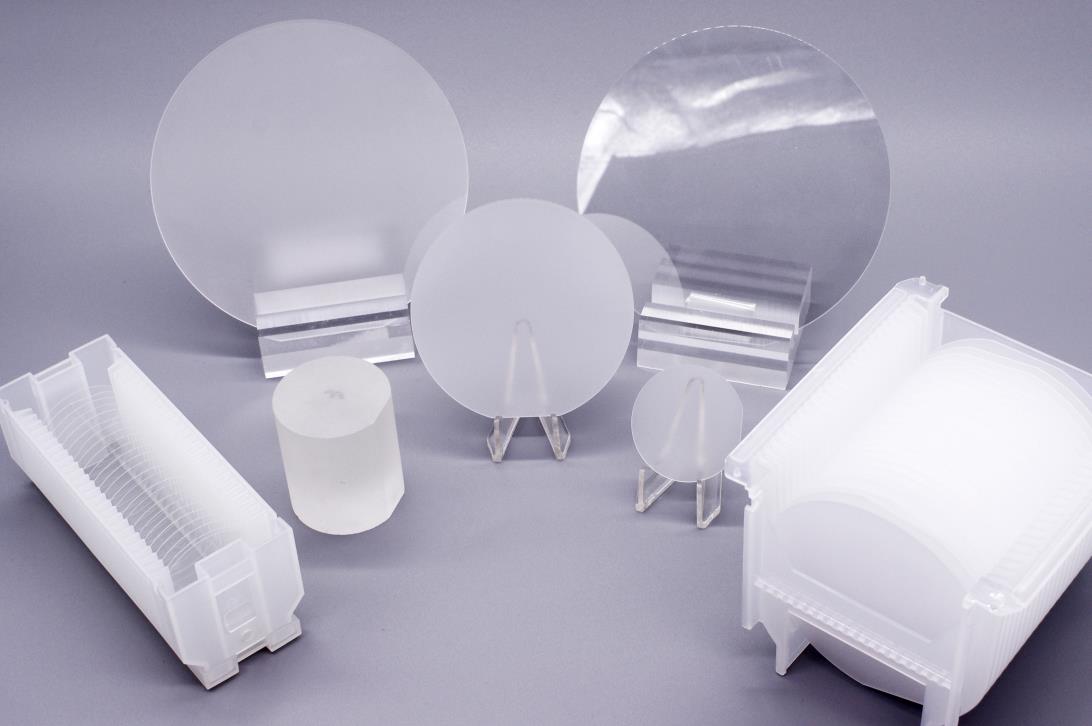
Saphire Wafers

We are happy to supply you with sapphire wafers with very low surface roughness in all orientations (C- A- R- M-Plane) up to a diameter of 200mm. The growing method can be HEM or Kyropolos.

We will be happy to advise you on individual requirements or the selection of the right specifications for your application.

Please call us on +49-(0)8191-478747 or contact us by per e-mail.

We can offer you the following sapphire wafers

Sapphire Wafers

Sapphire wafers are monocrystalline substrates made from synthetic sapphire, a crystalline aluminum oxide (Al2O3).

These wafers are produced by a process called liquefaction zone growth, in which aluminum oxide is melted in a high-temperature furnace and then solidifies into a single crystal under controlled conditions. Sapphire wafers are characterized by their hexagonal crystal structure, high hardness, chemical resistance and transparency in the visible and infrared range. They are used in the semiconductor industry, optoelectronics and other high-tech applications as substrates for the production of LEDs, optical components and sensors.

Kyropolos

In the Kyropolos method, sapphire is extracted from a melt by crystallization. The process involves melting high-purity aluminium oxide (Al2O3) and then crystallizing the molten material while it is slowly cooled. This forms large sapphire crystals, which are then cut into slices and polished to produce sapphire wafers. The Kyropolos method enables the production of sapphire wafers with high purity and crystal quality, making it ideal for applications that require a uniform structure and high transparency, such as in the optoelectronics and LED industries.

HEM (Heat Exchanger Method)

HEM (Heat Exchanger Method):
The HEM method for producing sapphire wafers involves crystallizing sapphire from a liquid aluminium oxide mixture, which is cooled by heat transfer from a heating medium. This leads to the formation of sapphire crystals at the interface between the melt and the cooling medium. Compared to the Kyropolos method, the HEM method enables faster crystallization and a higher production rate. However, the sapphire wafers produced in this way can have a lower crystal quality and may not be as uniform as with the Kyropolos method.

C-A-R-M

C-A-R-M stands for the Miller indices of the crystal axes in the hexagonal structure of sapphire. The letters correspond to the axis directions [1-100], [11-20], [1-102] and [1-101]. The “C-A-R-M plane” refers to a specific crystal plane within the sapphire crystal, which is defined by the arrangement of the atoms along these axes. This crystal plane can be important for certain applications in the semiconductor industry, optoelectronics and other fields, as it can influence certain properties of the sapphire wafer, such as the electrical, optical or mechanical properties.

Areas of application for our sapphire wafers (silicon-on-sapphire, SOS)

Semiconductor industry

Sapphire wafers are used as substrates for the production of light-emitting diodes (LEDs) and laser diodes.

Electronics

Sapphire wafers are used in microelectronics for the manufacture of high-frequency and high-performance electronic components such as high-performance transistors and high-frequency circuits.

Optics

Due to their optical properties, sapphire wafers are used for windows, lenses and optical components in various applications such as cameras, lasers and sensors.

Watch industry

Sapphire glass is often used as a scratch-resistant material for watch crystals.

Typical sapphire wafer specifications:

Diameter:
50,8mm
76,2mm
100mm
125mm
150mm
200mm

Growth:
Kyropolos
HEM

Orientation:
C-Plane (0001)
A-Plane (11-20)
R-Plane (1-102)
M-Plane (10-10)

Surface/ Finish:
Optical Polished
EPI Polished
Fine Ground
As Lapped

Roughness:
Polished <= 0,3nm
Fine Ground <1 μm
As Lapped <1 μm